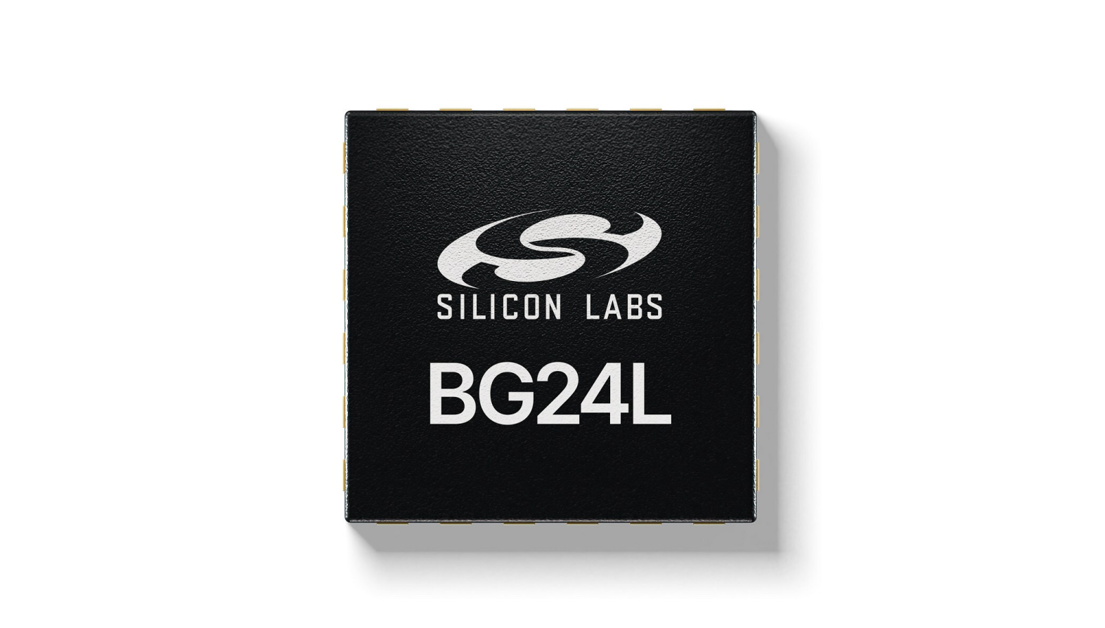
The BG2B represents the company’s most power-efficient Bluetooth architecture to date, achieving a 14% to 15% reduction in MCU active current compared to previous generations. With a sleep current of 1.1 µA while maintaining RAM, the chip is engineered for devices that spend most of their life in low-power states, such as smart locks, electronic shelf labels, and asset trackers.
Beyond power savings, the SoC addresses the growing demand for precise location awareness by incorporating Bluetooth Channel Sounding. The hardware supports Mode 3, Normalized Attack Detector Metric, and Inline Phase Correction Term, aligning with specifications from Apple and Google. To reduce total system costs, Silicon Labs integrated CAN-FD, dual 12-bit ADCs, and LED drivers directly onto the die, effectively shrinking the required bill of materials and physical PCB footprint.
Security remains a focal point, as the BG2B utilizes Secure Vault High technology to meet PSA Level 3 compliance. This architecture enables manufacturers to address looming regulatory mandates, including the European Union Cyber Resilience Act, by protecting cryptographic keys and firmware from inception. While the SoC is currently accessible through an early customer engagement program, Silicon Labs expects to transition to initial production hardware and modules by 2027.




Comments (0)
No comments yet. Be the first!