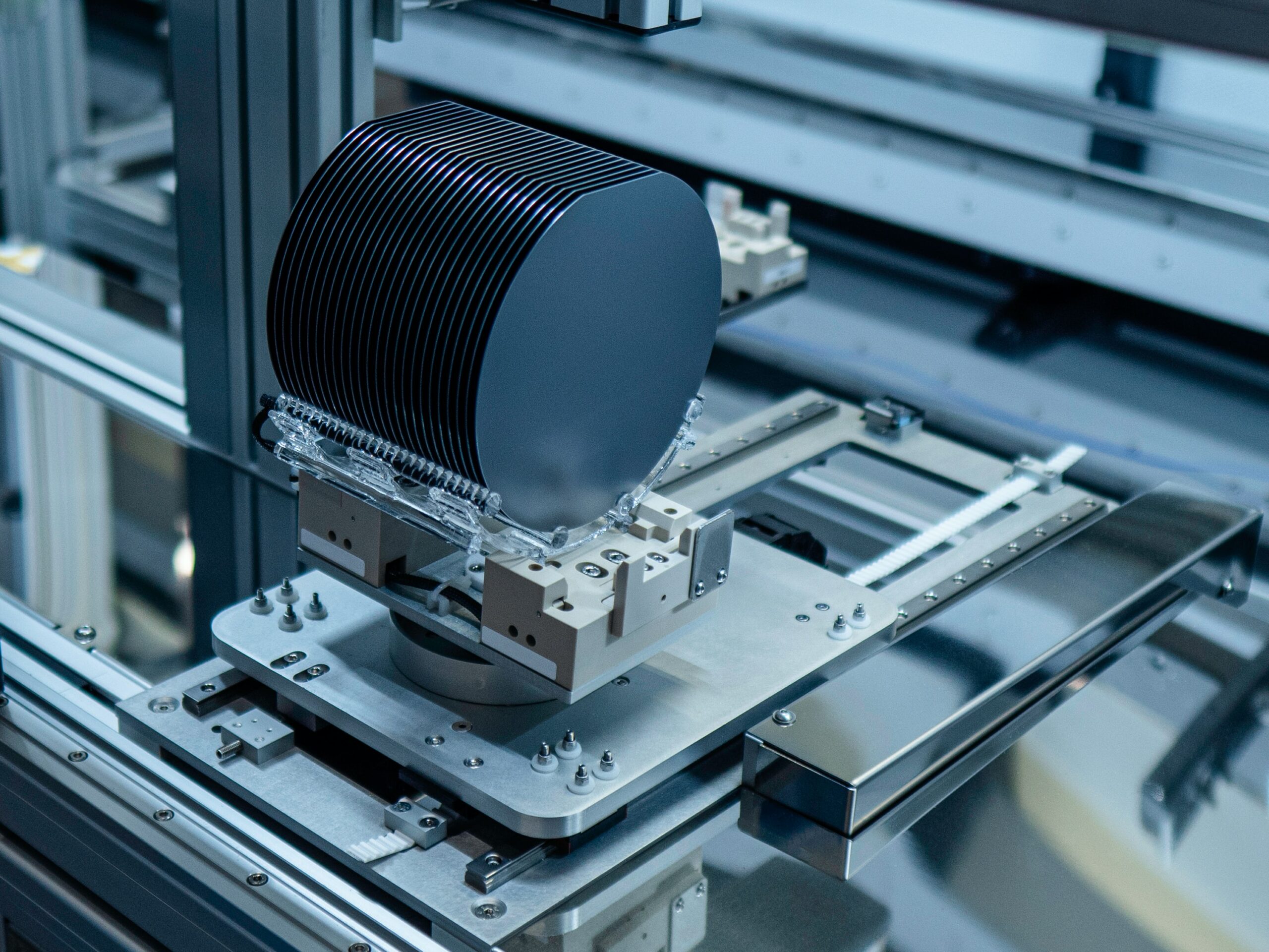
The exhibition serves as a strategic push into India’s rapidly maturing semiconductor landscape, where government backing and increased local design activity are driving demand for specialized manufacturing. DB HiTek plans to highlight its flagship BCD process, which has already surpassed 9 million cumulative wafer shipments, alongside its push into automotive and industrial applications.
Technological development remains central to the company’s expansion strategy. DB HiTek recently finalized process qualification for its 1,200V SiC MOSFET and expects to complete testing for its 650V GaN process by the end of this year. These next-generation power technologies are currently undergoing performance evaluations with strategic partners. Beyond power semiconductors, the foundry will promote its specialty CIS capabilities, including SPAD and global shutter technologies, aiming to capture a broader share of the Indian market’s emerging design sector.



Comments (0)
No comments yet. Be the first!